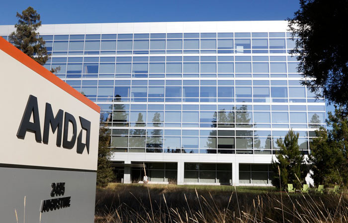
Low-vibration & low-noise building design Structural & FEA modeling MEP vibration isolation
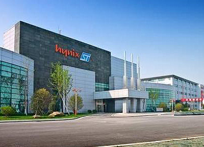
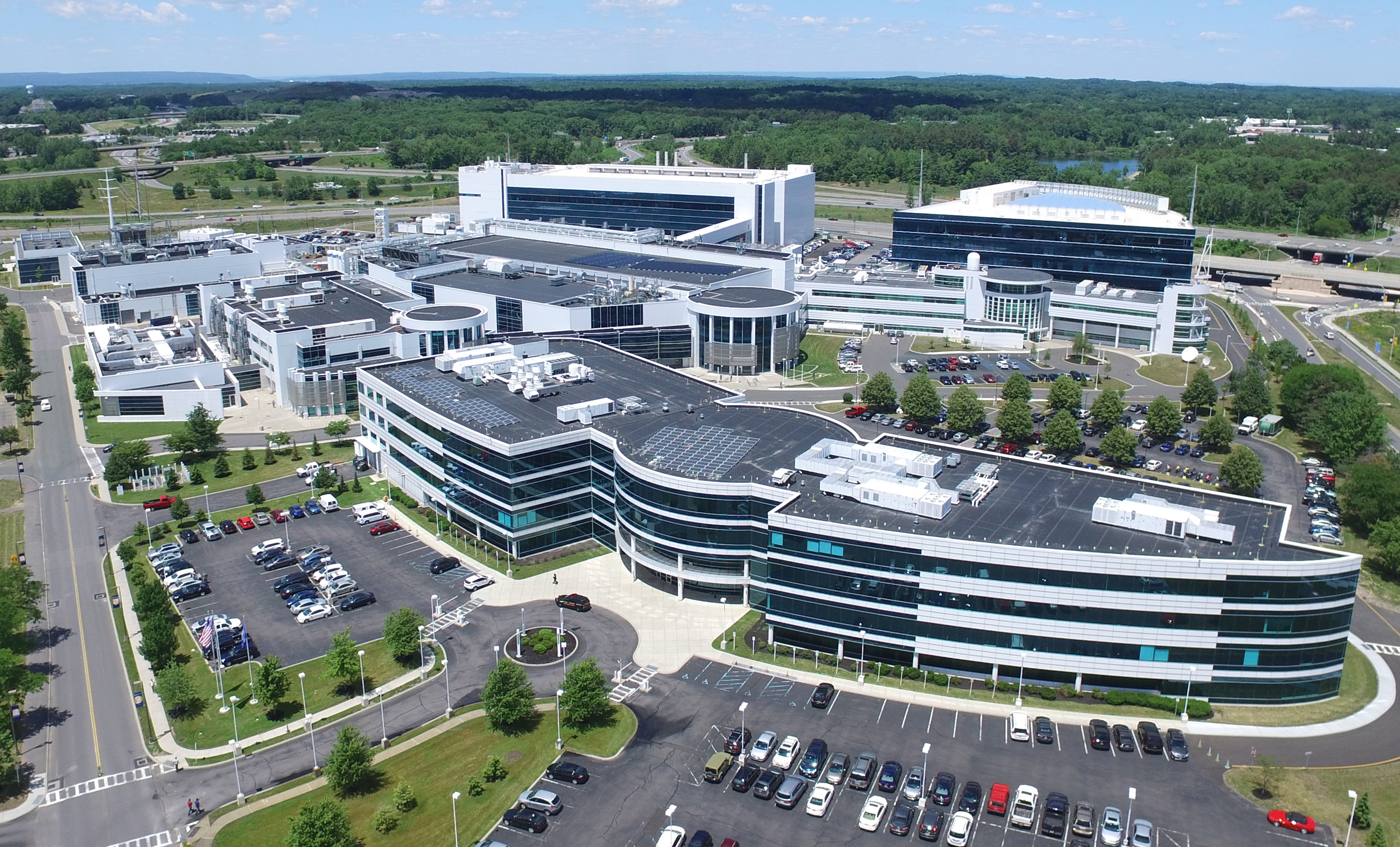
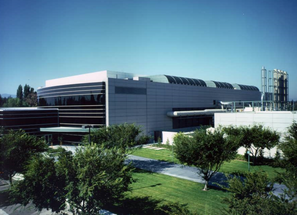
This is the first Hynix fab in China. The facility will be capable of manufacturing 300mm wafers with sub-0.1 micron geometry for both DRAM and NAND flash memories. The master plan anticipates a total of four fabs at this site. 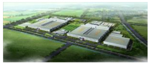 One pair of mirror-image fabs (sharing a central core building) was constructed as shell during the first phase of construction. One side was designed for 200mm technology; the other side for the most advanced 300mm technology. Failure Analysis (FA) labs are located in the support building at the ground floor. The site includes a probe/test building, CUB, dormitories/cafeterias, and warehouse space. As of the initiation of the project, this is the largest semiconductor manufacturing complex in China.
Our lateral system design makes use of eight stair towers along two opposing edges and two stair towers along the short edges as boxed shearwalls. This lateral design
allowed us to eliminate all interior shearwalls, resulting in major construction cost savings and improvement in flexibility in subfab space-utilization.
Services Provided:
• Site Ambient Vibration Survey
• Structural Vibration Design, Finite Element Analyses
• Mech/Elec/Plumbing equipment Vibration Isolation
• Provide Sound Power Requirements
• At-rest Structural Vibration and Noise Evaluation


